Engineering Innovation
to Manufacturing Reality
From concept to production — integrated electronics, software, & mechanical manufacturing at a cost effective price.
AS9100 Rev. D Certified • ITAR Registered • IPC Class 3 Capable • CAGE: 750L8
Our Core Services
Full-spectrum engineering and manufacturing under one roof.
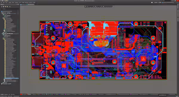
PCB Design & Layout
Multi-layer PCB design and layout optimized for manufacturability, signal integrity, and thermal performance.

PCB Assembly
High-quality surface mount and through-hole assembly with AOI, X-ray inspection, and functional testing.
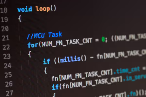
Firmware Development
Custom firmware for embedded systems, microcontrollers, and FPGA platforms.
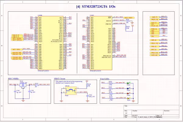
Circuit Design & Schematic Capture
Expert circuit design and electronic systems development from concept through production.
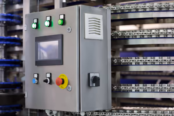
Enclosure & Box-Build
Custom enclosure fabrication and full system integration with wire harness assembly.

Mechanical Fabrication
Precision sheet metal fabrication, CNC milling, and custom mechanical components.
PCB Design & Layout
Multi-layer PCB design and layout optimized for manufacturability, signal integrity, and thermal performance.
PCB Assembly
High-quality surface mount and through-hole assembly with AOI, X-ray inspection, and functional testing.
Firmware Development
Custom firmware for embedded systems, microcontrollers, and FPGA platforms.
Circuit Design & Schematic Capture
Expert circuit design and electronic systems development from concept through production.
Enclosure & Box-Build
Custom enclosure fabrication and full system integration with wire harness assembly.
Mechanical Fabrication
Precision sheet metal fabrication, CNC milling, and custom mechanical components.
TRUSTED // BY
Our Clients


SECTORS // WE SUPPORT
Built for Every Industry

Aerospace
Flight-critical avionics and satellite electronics built to AS9100 standards.

Defense & Military
ITAR-registered manufacturing for mission-critical defense systems.

Medical Devices
IPC Class 3 assemblies for diagnostic and life-support equipment.

Industrial
Ruggedized electronics for automation, robotics, and heavy machinery.

Commercial
Scalable electronics for office, retail, and building automation systems.

Communications
High-frequency RF and signal processing for telecom infrastructure.

Consumer Devices
Compact, cost-optimized boards for consumer electronics at scale.

Green Energy
Power conversion and control systems for solar, wind, and EV charging.

LED Lighting
Custom LED drivers and control circuits for commercial lighting.

Transportation
Durable electronics for automotive, rail, and marine applications.
OUR // DIFFERENCE
Why Choose Calpak USA
40+ years of American engineering — making "Going Onshore" our blueprint for the future.
AS9100 Rev. D Certified
Concept to Production Under One Roof
ITAR Registered & ESD Controlled
Trusted Supply Chain Partnerships
Cost-Optimized Engineering
Made in Hawthorne, California
PROCESS // OVERVIEW
How It Works
From first call to ongoing support — a streamlined path to production.

Consult & Scope
Share your requirements and objectives. We assess feasibility, define specifications, and outline a clear project roadmap — ensuring alignment before any work begins.

Design & Develop
Our engineers create schematics, PCB layouts, firmware, and mechanical designs — iterating closely with your team until every detail is production-ready.

Build & Assemble
We manufacture with IPC Class 3 workmanship and AS9100 quality assurance. Surface mount, through-hole, and full system integration — all under one roof.

Test & Verify
Every unit undergoes AOI inspection, X-ray analysis, and functional testing to ensure it meets your exact specifications before leaving our facility.

Ship & Support
Final packaging, logistics coordination, and ongoing technical support for the lifetime of your product. We stay with you from prototype through full-scale production.
Common Questions
Frequently Asked Questions
What is included in a PCB assembly quote from Calpak USA? +
A Calpak USA PCB assembly quote covers every cost element so there are no surprises at invoicing. The quote itemizes bare board fabrication, component procurement with line-by-line pricing, solder paste stencils, SMT and through-hole assembly labor, any required programming or conformal coating, inspection (AOI, X-ray for BGAs), functional testing, and packaging. Calpak USA also flags potential cost risks such as long-lead or allocated components and offers alternates where possible. NRE charges for stencils, fixtures, and test development are broken out separately. Quotes are typically returned within 3 to 5 business days from our Hawthorne, California facility once we receive Gerber files, a BOM in spreadsheet format, and assembly drawings. Requesting a quote carries no obligation, and our engineering team is available to review your documentation before formal submission. For a detailed breakdown of every line item and tips on reducing cost, see our PCB Assembly Quote Guide.
How does Calpak USA handle component shortages or obsolescence during procurement? +
Calpak USA actively monitors component lifecycle status during every procurement cycle. When a part is flagged as end-of-life, allocated, or on extended lead time, our supply chain team notifies your engineering contact immediately with documented alternates that match the original specifications for package, tolerance, and operating range. Calpak USA cross-references parts through authorized distributors, manufacturer franchise networks, and vetted independent sources that meet our AS9100 Rev. D incoming inspection requirements. For defense programs, all substitutions require customer-approved deviation authorization before placement. We also offer last-time-buy planning and long-term inventory stocking agreements for programs with multi-year production forecasts. This proactive approach, managed from our Hawthorne, California facility, minimizes line-down risk and keeps your production schedule on track.
What certifications should I look for when choosing a contract electronics manufacturer? +
The certifications you require depend on your end market. For aerospace and defense programs, look for AS9100 Rev. D (aerospace quality management), ITAR registration (export-controlled defense articles), and IPC Class 3 assembly capability (high-reliability solder joints). For commercial and industrial products, ISO 9001 and IPC Class 2 are standard benchmarks. ANSI/ESD S20.20 certification confirms proper electrostatic discharge controls throughout the facility. Calpak USA holds all of these certifications and maintains them through annual third-party audits. Our Hawthorne, California facility is also equipped for J-STD-001 compliant soldering with both leaded and lead-free processes. When evaluating a contract manufacturer, request copies of current certificates and ask about the scope of coverage, as some CMs only certify a subset of their operations.
What is the difference between IPC Class 2 and IPC Class 3 PCB assembly? +
IPC Class 2 is the standard for dedicated-service electronic products such as industrial equipment and commercial hardware. It permits minor cosmetic imperfections that do not affect form, fit, or function. IPC Class 3 is the high-reliability standard required for aerospace, defense, medical life-support, and mission-critical systems where continuous performance and long service life are mandatory. Class 3 imposes tighter requirements on solder fillet size, heel wetting, barrel fill for through-hole joints, and acceptable levels of voiding in BGA solder balls. Calpak USA assembles to both IPC Class 2 and Class 3 standards at our Hawthorne, California facility, with IPC-certified operators and inspectors on every production line. Your purchase order or drawing notes determine which class applies, and Calpak USA documents compliance with full inspection records per AS9100 Rev. D traceability requirements. For a complete comparison of Class 2 vs. Class 3 acceptance criteria, see our IPC Class 3 Assembly Guide.
Can Calpak USA support both prototype and high-volume production from the same facility? +
Yes. Calpak USA operates dedicated prototype and production assembly lines within our single Hawthorne, California facility, supporting volumes from one board through 10 million units per year. Prototype builds use the same equipment, solder processes, and IPC workmanship standards as production, so your validation results translate directly to volume manufacturing without process requalification. When a design moves from prototype to production, Calpak USA retains all tooling, stencils, test fixtures, and process documentation, eliminating NRE duplication and reducing ramp time. Our engineering team manages the transition, addressing any DFM refinements identified during prototyping before the first production lot. This single-facility model also simplifies vendor qualification for quality systems that require AS9100 Rev. D or ITAR compliance across the full product lifecycle.
What files and documentation does Calpak USA need to start a PCB assembly project? +
Calpak USA requires three core deliverables to begin quoting and production planning. First, Gerber files (RS-274X or ODB++ format) including all copper layers, solder mask, silkscreen, paste layers, drill files, and a board outline. Second, a bill of materials in spreadsheet format with manufacturer part numbers, descriptions, reference designators, quantities per board, and any approved alternates. Third, assembly drawings showing component placement, polarity indicators, keep-out zones, and any special instructions such as selective soldering or conformal coating boundaries. Additional helpful documents include a netlist for test development, a schematic for functional test reference, and any IPC class or workmanship callouts. Calpak USA reviews all submitted files at our Hawthorne, California facility and provides a DFM report before assembly begins, flagging potential issues with pad geometry, component spacing, or thermal relief.
How does Calpak USA protect intellectual property and ITAR-controlled technical data? +
Calpak USA maintains strict IP and data security protocols across our Hawthorne, California facility. All customer design files, BOMs, test procedures, and firmware are stored on access-controlled servers with role-based permissions. ITAR-controlled technical data is handled exclusively by U.S. persons in compliance with our registration with the Directorate of Defense Trade Controls. Non-disclosure agreements are executed before any proprietary data is exchanged. Physical facility access is controlled with badge entry, visitor logs, and escorted access policies for non-employees. Calpak USA does not share customer data with third parties without written authorization, and our AS9100 Rev. D quality system includes documented procedures for data handling, retention, and destruction. For programs requiring additional cybersecurity measures, Calpak USA can implement customer-specified data handling protocols upon request.
What is DFM review and does Calpak USA provide it before assembly begins? +
Design for manufacturability review is an engineering analysis of your PCB layout, BOM, and assembly drawings to identify issues that could cause yield loss, assembly defects, or reliability problems before a single board is built. Calpak USA performs a DFM review on every project at no additional charge. Our engineers check pad geometries against IPC-7351 land pattern recommendations, verify solder paste stencil aperture ratios, evaluate component spacing for rework access, flag thermal imbalances that cause tombstoning on passive components, and confirm BOM part availability. The DFM report is returned as a documented package with annotated images and recommended corrections. Calpak USA does not proceed to assembly until all flagged items are resolved or formally accepted by your engineering team. This process, standard at our Hawthorne, California facility, consistently reduces first-pass defect rates and avoids costly rework cycles. For a complete DFM checklist and common mistakes to avoid, see our PCB Design for Manufacturing Guide.